Buy Electronic Components Online
All about Vias
A printed circuit board may have a number of holes for different purposes. Some holes may be for mounting the board on or inside an appliance, while others for orienting and locking a component such as an LCD or a connector on the PCB. The PCB may have slots for improving air circulation or providing increased insulation, and holes in PCB panels typically for helping to separate multiple PCBs. Apart from all the above, a multi-layer PCB will usually have extremely small holes or vias, which help in connecting circuits in its different layers.
A via is typically a hole in the multi-layer PCB with a few pads on different layers of the board electrically connected by a conductive tube passing through the hole. During fabrication of the PCB, a process of electroplating, whereby a thin layer of copper is deposited on the walls of the hole and connecting the two pads forms the conductive tube.
Different Types of Via
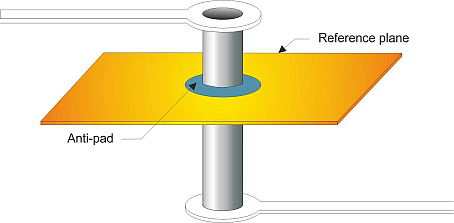
Each via consists of three parts—Barrel, Pads, and Antipads. The barrel is the conductive tube filling the hole and formed by electroplating. Pads at both ends of the barrel connect it to a components, planes, or traces. If the barrel has to pass through a plane without connecting to it, the antipad forms the clearance between the barrel and the metal layer.
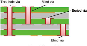
Some vias may have to pass through all the layers of a multi-layer PCB and its pads appear on circuits on both the outer surfaces of the board. These are the plated through holes or PTH vias. While passing through the board, some inner planes or circuits may connect to the PTH via, if necessitated by the electrical requirements of the schematic.
Some vias originate on one of the outer surfaces of a multi-layer PCB but terminate on an inner layer, so only one of the pads is visible. These are blind vias and apart from the two extreme layers, they may connect to some intermediate layer as well, again, only if there is a requirement.
Fabricators may have to embed some vias totally inside a multi-layer PCB. These buried vias connect two or more circuits on the inner layers of the PCB, and are not visible from the outside. Fabricators incorporate blind vias when assembling the PCB layer by layer and it is impossible to introduce them once the PCB has been stacked up.
Sometimes vias may be placed on the common edge of two boards in a panel, so that separating the two boards causes the via to be cut into two parts, one-half on each board. These are castellation vias and useful for soldering the PCB to a connector.
Application of Vias
The main function of a via is to electrically bridge some sections of the circuit present on different layers, while bypassing other circuits. By placing vias at strategic places, the designer can make the entire circuit fit within a few layers of a multi-layer PCB. Not only does this reduce the physical dimensions of the PCB, it brings additional benefits such as cost reduction, better signal integrity, and improved reliability.
Mounting fine pitch components on PCBs would be practically impossible if not for vias. Fine pitch components such as BGAs with pitch less than 0.5 mm do not have enough space between pads to allow multiple fine traces to run through them. The only option a designer has for breaking out traces from such closely spaced pads is to use vias placed directly on the pads. However, these vias must be filled and tented to prevent solder wicking.
Dense PCBs with very fine traces may not have much space available for placing vias with pads. Therefore, engineers have to use landless vias. These are vias without the customary pads, placed in the middle of a trace, often with a diameter matching the trace width.
With the increasing demand for fine pitch components and high density PCBs, designers require vias with very small diameter. Beyond a certain stage, drilling holes with mechanical drill bits becomes impossible. Fabricators then drill microvias with laser beams, as these can drill holes of about 25-35 µm in diameter. These small vias leave adequate space for routing traces.
Designing a PCB with Vias
Almost all designers nowadays use a computerized tool to design their PCBs. The library of these CAD tools usually have standard via design symbols built-in. As the pad diameter bears a relation to the hole diameter, specifying the hole diameter of the via allows the CAD tool to place appropriately sized pads and antipads on specific layers.
The designer usually begins by arranging all the components on the surface of the PCB, after defining the mechanical constraints such as the PCB outer dimensions and others such as the mounting holes. The net list from the schematic capture usually guides the auto-router CAD tool in interconnecting the component pads. If the tool is unable to find a direct route on the layer, it will try a route through another layer, placing vias to descend to an inner layer and subsequently, to return to the first. For optimal routing, the designer may have to move the position of the via from its present coordinates defined by the auto-router.
Necessity for a Via
The primary reason for a designer needing a via is to make use of the inner layers for routing signals and power in a multi-layer PCB—it is not possible to do so from the top surface layers without using a via. Likewise, vias are a necessity when breaking out the connections from a fine-pitch component such as a BGA.
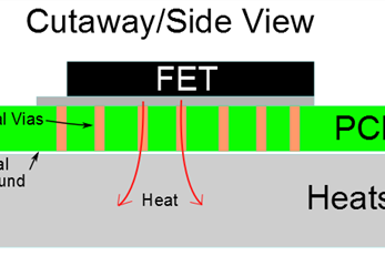
However, vias also serve another important function—that of heat removal. As manufacturers shrink IC dimensions, removing the heat build-up from inside the package to the external environment becomes more difficult. To help dissipate the heat, manufacturers provide a metal tab on the underside of the IC package, and this tab connects directly to the IC chip within the package. In most cases, the metal tab is electrically isolated, and has only a thermal connection to the IC chip.
The designer has to provide a copper land at the position where the IC package will sit on the PCB, so it is in touch with the metal tab under the IC. In operation, as the IC and the metal tab heat up, the copper land conducts heat away from the metal tab, thereby keeping the IC within its operating temperature range.
However, the copper land is usually very thin and therefore, unable to transfer heat efficiently. The designer has to assist the heat transfer by placing a thicker layer of copper on the opposite side of the PCB. A copper or aluminum heat sink attached to this thick copper then efficiently transfers the heat to the surrounding environment.
The designer connects the copper land under the IC and the thick copper on the opposite side of the PCB by placing multiple vias between them. Usually, fabricators fill these vias with copper so they transfer heat better.
DFM for Vias
Adhering to Design for Manufacturing (DFM) guidelines helps avoid pitfalls usual during the design of PCBs that cause a hold up in PCB production, as the fabricator finds the design is liable to fail in the manufacturing processes. There can be many reasons for this, and the DFM review should weed out the issues before the PCB documents reach the fabricator.
When checking vias, DFM reviewers primarily measure several via parameters and compare them against pre-defined tolerances. Major parameters they check are:
- Minimum drill hole diameter
- Minimum finish hole diameter
- Controlled depth for blind and buried vias
- Minimum outer layer annular ring
- Minimum inner layer annular ring
- Drill to plane clearance
- Maximum aspect ratio
- Diameter tolerance
- Location tolerance
When checking the relationship of a via to the rest of the circuit surrounding it, the parameters DFM reviewers check are:
- Registration tolerances
- Minimum webbing between solder masks
- Via clearance of solder mask
- Encroachment of solder mask onto via
- Anti-pad and plane relief
- Thermal relief
Apart from the above, there may be requirements for fabricators to plug, fill, or tent vias on a PCB. DFM reviewers will check whether unambiguous instructions exist for the fabricator to comply with the requirements.
It is typical for PCBs to have tooling holes and fiducial marks to assist in various stages of manufacture. DFM for vias should include the positional tolerances of vias from tooling holes and fiducial marks.
PCBs manufactured in panels typically use perforated breakaway tabs, v-groove breakaway tabs, or may need separation by hand cutting or machine shearing. DFM reviewers will check for minimum clearance of traces and vias from the routed/scored edges. Additionally, the solder side of the PCB should have a minimum clearance on both sides along the long edge of the PCB, to allow the carrier fingers hold the PCB during transportation. No via or component is allowed in this clearance zone.
DFM reviewers will also check the position of vias for BGA packages. If the designer has used via-in-pad design, the instruction for these vias should include filling and tenting them. For dog-bone designs, the designer should preferably separate each via from its pad with a predefined short trace covered with solder mask.
Finally, specifically for vias, the board documentation should include a drill file with tool codes and X-Y coordinates for all holes. The fab drawing should include a drill chart with hole symbols on the drawing and finished hole sizes. The Gerber files should include via plugging holes if required.
Top 10 High Quality Power Stencils in India, PCB Manufacturing Services, Turnkey PCB Manufacturer in India, PCB Prototype Manufacturer, PCB Fabrication and Assembly, PCB Cost Calculator, Buy Electronic Components Online, High Frequency Power Stencils in India, PCB Fabrication Services in India, Printed Circuit Board in India, Fabrication PCB, PCB Board, PCB Production, PCB Order, PCB Prototype, PCB Manufacturer, PCB Prototype Manufacturer, PCB Prototype Assembly, PCB Low Cost, PCB Prototype Fabrication, PCB Manufacturing, PCB Prototype Low Cost, Prototype PCB Board Manufacturer, PCB Manufacturing Service, Prototype Circuit Board Manufacturers, Cest PCB Prototype Service, PCB Manufacturing in India, PCB Fabrication Process, PCB Board Material, How to use Printed Circuit Board, How to use PCB Fabrication, PCB Online calculator, PCB Electronic Circuit Board, PCB Assembly Process, PCB Online Store, PCB Component Sourcing Material, PCB Power, PCB Power Login, PCB Manufacturing, PCB Fabrication, PCB Online, Online PCB design, PCB Power supply, PCB electronics, PCB design India, PCB Board price in India, PCB Service, PCB Maker, PCB Stencil, Power Circuit Board, PCB Printing Service, Custom PCB, PCB India, PCB Manufacturing Cost, PCB Order, PCB Online Quote, Buy PCB