PCB Board
Relationship between Solder Wicking and Surface Finish
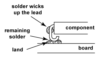
During reflow, the solder paste may tend to wet the component termination rather than both the printed circuit board (PCB) pad and the lead, as it should do normally. This phenomenon is called solder wicking, and the main reason for this is the slow wetting of the pad or a much faster wetting of the termination.
Faster Wetting of the Termination
The reflow profile or the soldering process is the main cause of faster wetting of the component lead. For instance, vapor phase can allow the leads to reach soldering temperatures much before the surface of the PCB can. Another contributor to wicking is the old tin/lead coated termination in a lead-free process. As the melting point of tin/lead coating is lower, the surface coating wets very quickly. The result literally sucks solder up the lead before it can even start to wet the pad on the PCB. Although in most cases the joint is satisfactory, larger component leads may carry the solder up, creating incomplete joints.
Slow Wetting on the Pad
Most lead-free alloys have reduced wetting characteristics, and the alternative surface finishes exaggerate these characteristics. Manufacturers improve the solderability performance of the PCB surface by coating them with other metals. A coating of solder offers the best solderability, followed by gold, silver, tin, and copper OSP. Of course, this is based on the specification, quality, and consistency of the finish provided. Several factors may contribute to the degree of surface coverage. Engineers need to optimize their reflow process for obtaining the best performance from the PCB.
Surface Finish Affects Wetting
In general, the amount of lead-free solder wicking depends on the surface finish of the pad and the finish of the component lead. This may result in unsoldered areas, and may result in solder displacement to areas close to the joint with the potential to create shorts. De-wetting may also cause solderability problems, where solder joints can be made and then destroyed by inappropriate soldering conditions.
Usually, manufacturers preserve the solderable surface of the PCB using a surface finish or coating as the PCB moves from manufacturing to assembly. The most common surface finishes offering the best solderability are, in order of preference, Hot Air Solder Leveling or HASL, Electroless Nickel/Immersion Gold or ENIG, Immersion Silver or ImAg, Immersion Tin or ImSn, and Organic Solderability Preservatives or OSP.
HASL—Hot Air Solder Leveling
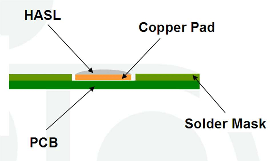
As a solder coating, HASL is available for both lead and lead-free PCBs. The application process involves pre-cleaning the exposed copper surface, preheating it, and flux coating it, before giving it a coating of solder. Excess solder is removed and the surface leveled by a hot-air knife. Typical thickness of the HASL layer is usually about 100-500 micro-inches.
Although HASL offers long shelf life, reliability, and very good solderability due to its short wetting time, it can lead to several undesired side effects. HASL may cause uneven surfaces or planarity issues and PTH diameter issues and bridging for fine pitch prints. The PCB may face a thermal shock due to the HASL process, and this may cause PCB warpage.
ENIG—Electroless Nickel/Immersion Gold
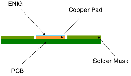
This is a plating of nickel over the exposed copper pad and a plating of gold over the nickel surface. The application process involves cleaning the exposed copper surface with micro-etching and depositing the electroless nickel over it. A plating of immersion gold then covers the nickel surface. The typical thickness of the nickel layer is 50-150 micro-inches, while the gold thickness is about 3-10 micro-inches.
As the gold surface does not oxidize, it offers long shelf life and good wettability and solderability. However, there are side effects also, such as nickel corrosion leading to black pads, and thick gold surface causing embrittlement. Additionally, slow intermetallic growth of nickel may lead to poor joint strength and reliability. ENIG is an expensive and complicated process, which, if not done right may aggravate non-wetting issues.
ImAg—Immersion Silver
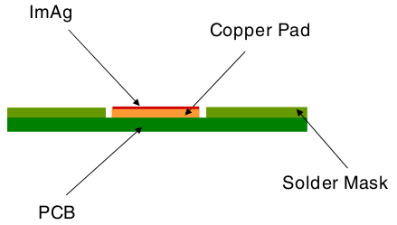
Immersion silver of 3-12 micro-inch thickness covers the exposed copper pad on the PCB, which has been cleaned and micro-etched prior to the application of the immersion silver.
Although immersion silver finish is low cost and produces a planar surface of high conductivity, it is subject to creep corrosion, planar micro voids, migration of silver, and tarnishes easily.
ImSn—Immersion Tin
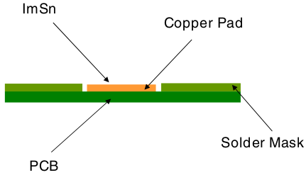
Manufacturers often protect the exposed copper pads on the PCB with a deposit of a thin layer of immersion tin. This low cost protection is low cost and produces a uniform surface of good solderability. However, many solder mask materials and plating chemicals attack immersion tin. Tin forms whiskers, which tend to create shorts, and it also forms solid state IMC.
OSP—Organic Solderability Preservatives
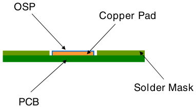
OSP is a transparent organic material coating, which manufacturers use to prevent the exposed copper pads from tarnishing. The applied thickness is usually 0.3-0.5 microns, and it forms an intermetallic bond with the copper surface.
The OSP application process is low cost, easy, and short. Although it produces a flat planar surface of good reliability, it produces the least solderability among all the above surface finishes. It has a short shelf life, and does not withstand multiple reflows.
Solving Solder Wicking in Reflow Soldering

As soldering is a complex science, various soldering processes have some common underlying issues and a few unique ones that need to be overcome for achieving a good solder joint. Solder wicking is one such serious problem where the issue is of solder climbing up on to the lead of a component. The root cause and mechanism of solder wicking are:
- The lead reaching the liquidus temperature before the pad does, tightens up the molten solder completely
- The hotter surface attracts the solder alloy, provided there is sufficient wettability
- Solder on the leads melts faster than on the solder joint—the enhanced liquefaction of solder at the lead pulls the melting solder paste away from the pads
- Wicking-up is aided by all non-wetting problems such as plating too thin, contamination/oxidation, or surface treatment
Experiments with 8-zone reflow ovens have demonstrated good solutions to the problem of solder wicking. Most effective settings for the oven were five pre-heat zones, and three peak zones, along with forced convection airflows. Such reflow ovens were capable of suitably processing very complex boards with optimum process stability and offered unmatched reproducibility.
Top 10 High Quality Power Stencils in India, PCB Manufacturing Services, Turnkey PCB Manufacturer in India, PCB Prototype Manufacturer, PCB Fabrication and Assembly, PCB Cost Calculator, Buy Electronic Components Online, High Frequency Power Stencils in India, PCB Fabrication Services in India, Printed Circuit Board in India, Fabrication PCB, PCB Board, PCB Production, PCB Order, PCB Prototype, PCB Manufacturer, PCB Prototype Manufacturer, PCB Prototype Assembly, PCB Low Cost, PCB Prototype Fabrication, PCB Manufacturing, PCB Prototype Low Cost, Prototype PCB Board Manufacturer, PCB Manufacturing Service, Prototype Circuit Board Manufacturers, Cest PCB Prototype Service, PCB Manufacturing in India, PCB Fabrication Process, PCB Board Material, How to use Printed Circuit Board, How to use PCB Fabrication, PCB Online calculator, PCB Electronic Circuit Board, PCB Assembly Process, PCB Online Store, PCB Component Sourcing Material, PCB Power, PCB Power Login, PCB Manufacturing, PCB Fabrication, PCB Online, Online PCB design, PCB Power supply, PCB electronics, PCB design India, PCB Board price in India, PCB Service, PCB Maker, PCB Stencil, Power Circuit Board, PCB Printing Service, Custom PCB, PCB India, PCB Manufacturing Cost, PCB Order, PCB Online Quote, Buy PCB