PCB Production
Importance of Stencil for PCB Assembly
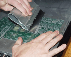
The surface mount assembly process uses a stencil as a gateway to an accurate and repeatable solder paste deposition. A stencil is a thin sheet or foil of brass or stainless steel with a circuit pattern cut into it, matching the positional pattern of surface mount devices (SMD) on the printed circuit board (PCB) for which the stencil is to be used. After accurately positioning and matching the stencil over the PCB, a metal squeegee forces solder paste through the apertures of the stencil to form deposits on the PCB for holding SMDs in place. The solder paste deposits, when passed through the reflow oven, melt and secure the SMDs to the PCB.
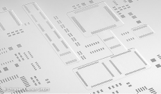
The design of the stencil, especially its composition and thickness and the shape and size of its apertures, determines the size, shape, and positioning of the solder paste deposits and this is crucial to ensuring a high-yield assembly process. For instance, the foil thickness and the aperture opening size define the volume of paste deposited on the board. An excess of solder paste causes balling, bridging, and tomb-stoning. Low amounts of solder paste cause dry solder joints. Both compromise the electrical functionality of the board.
Optimum Foil Thickness
The types of SMDs on the board define the optimum foil thickness. For instance, component packages such as 0603 or SOICs with a 0.020” pitch require rather thin solder paste stencils, whereas a thicker stencil is more suitable for components such as 1206 or SOICs of 0.050” pitch. Although stencil thickness for solder paste deposition ranges from 0.001” to 0.030”, the typical foil thickness that a majority of boards use ranges from 0.004” to 0.007”.
Technologies for Making Stencils
At present, the industry uses five technologies for making stencils—laser-cut, electroformed, chemically etched, and hybrid. While the hybrid technology is a combination of chemical etching and laser-cutting, chemical etching is very useful for making step stencils and hybrid stencils.
Chemical Etching for Stencils
Chemical milling etches metal masks and flexible metal mask stencils from both sides. As this etches not only in the vertical direction but also laterally, it causes undercutting, and makes the openings larger than desired. As the etching proceeds from two sides, the tapering on the straight wall causes the formation of an hourglass shape, leading to extra deposits of solder.
As etching the stencil openings does not produce a smooth result, the industry uses two methods for smoothening the walls. One of them is electropolishing, a microetchng process, and the other is nickel plating.
Although a smooth or polished surface helps paste release, it may also cause the paste to skip the surface of the stencil rather than roll with the squeegee. Stencil manufacturers address this problem by polishing the aperture walls selectively, but not the stencil surface. While nickel plating improves stencil smoothness and the printing performance, it reduces the aperture opening, which requires artwork adjustment.
Laser Cutting for Stencils
Laser cutting is a subtractive process, where Gerber data is fed to a CNC machine that controls the laser beam. The laser beam starts from inside the boundary of the aperture and traverses to its perimeter, while completely removing the metal to form the apertures, one aperture at a time.
Several parameters define the smoothness of the laser cut. This includes cutting speed, beam spot size, laser power, and beam focus. Typically, the industry uses a beam spot of about 1.25 mils, which cuts very accurate aperture sizes over a wide range of shape and size requirements. However, laser cut apertures also require post-processing treatments just as chemically etched apertures do. Laser cut stencils require electropolishing and nickel plating to smoothen the inside walls of the aperture. As the aperture size reduces during the latter process, the laser cut aperture size must be suitably compensated.
Aspects of Printing with a Stencil
Printing with a stencil involves three distinct processes. The first is the aperture-fill process where the solder paste fills the aperture. The second is the paste transfer process, where the paste accumulated in the aperture transfers to the PCB surface, and the third is the positional location of the deposited paste. The three processes are vital to achieving the desired result—depositing a precise volume of solder paste (also called a brick) to the correct location on the PCB.
Filling the stencil aperture with solder paste requires a metal squeegee blade forcing the solder paste into the aperture. The orientation of the aperture with respect to the squeegee blade affects the fill process. For instance, apertures oriented with their short axis in the direction of the blade stroke fill better compared to those with their long axis oriented to the blade stroke. Additionally, as squeegee speed influences aperture fill, lower squeegee speeds achieve better fills for apertures with their long axes oriented parallel to the stroke of the squeegee.
The edge of the squeegee blade also influences the way the paste fills the aperture of a stencil. The usual practice is to print applying minimum squeegee pressure while maintaining a clean wipe of the solder paste on the stencil surface. Increasing the squeegee pressure may damage both the squeegee blade and the stencil, while also causing paste smearing below the stencil surface.
Read Also: How to choose the correct PCB Material for your requirements?
On the other hand, lower squeegee pressure may not allow release of paste through a small aperture, resulting in insufficient solder on the PCB pad. Additionally, paste left on the side of the squeegee near large apertures will likely be pulled down by gravity, resulting in deposition of excess solder. Therefore, a minimum amount of pressure is necessary, which will achieve a clean wipe of the paste.
The amount of pressure to be applied also depends on the type of solder paste being used. For instance, Teflon/nickel-coated squeegee blades require about 25-40% more pressure when using lead-free solder paste than that required for tin/lead paste.
Performance Issues with Solder Paste and Stencils
Certain performance issues related to solder paste and stencils are:
- Thickness of the stencil foil and the aperture size determine the potential volume of solder paste deposited on the PCB pads
- The ability of the solder paste to release from the aperture walls of the stencil
- Positional accuracy of the solder brick printed on the PCB pad
During the print cycle, as the squeegee blade travels across the stencil, solder paste fills the stencil aperture. During the board/stencil separation cycle, the paste releases to the pads on the board. Ideally, all the paste that filled the aperture during the print process should have released from the aperture walls and transferred to the pad on the board, forming a complete solder brick. However, this transfer amount depends on the aspect ratio and area ratio of the aperture.
For instance, with an area of the pad greater than two-thirds the area of the inside aperture wall, the paste can achieve a release of better than 80%. This means reducing the stencil thickness or increasing the aperture size can give a better paste release with the same area ratio.
The ability of the solder paste to release from the aperture walls of the stencil also depends on the finish of the aperture walls. With electropolished and/or electroplated laser-cut apertures, the paste transfer efficiency improves. However, transfer of solder paste from the stencil to the PCB also depends on the adhesion of the paste to the aperture walls of the stencil and on the adhesion of the paste to the pad on the PCB. For a good transfer the latter should be greater, which means the printability depends on the ratio of the stencil wall area to the open face area, while ignoring minor influences such as the draft angle of the wall and its roughness.
The positional and dimensional accuracy of the solder brick printed on the PCB pad depends on the quality of the transferred CAD data, the technology and methods used to manufacture the stencil, and the temperature of the stencil during its use. Moreover, the positional accuracy also depends on the alignment methods used.
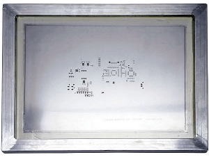
Framed Stencils or Glue-In Stencils
Framed stencils are the strongest form of laser-cut stencils available and are designed for high-volume screen-printing during production runs. These are permanently mounted in a stencil frame with a mesh border tightly stretching the stencil foil taut in the frame. Framed stencils with smooth aperture walls are recommended for Micro BGAs and for components with 16 Mil pitch and below. Framed stencils offer the best positional and dimensional accuracy when used under controlled temperature conditions.
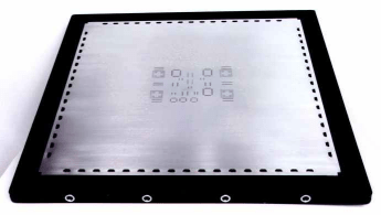
For short runs or prototype PCB assembly, frameless stencils offer optimum solder paste volume control. They are designed to work with a stencil tensioning system, which are reusable stencil frames such as universal frames. As the stencils are not permanently glued into a frame, they are significantly cheaper than framed stencils and take up considerably lower storage space.
Conclusion
For achieving good printing results with a stencil, a variety of factors must form a right combination. These include:
- The right paste material—correct metal content, viscosity, the largest powder size, and lowest possible flux activity
- The right tools—proper stencil, printer, and squeegee blade
- The right process—good registration, and clean sweep.
Top 10 High Quality Power Stencils in India, PCB Manufacturing Services, Turnkey PCB Manufacturer in India, PCB Prototype Manufacturer, PCB Fabrication and Assembly, PCB Cost Calculator, Buy Electronic Components Online, High Frequency Power Stencils in India, PCB Fabrication Services in India, Printed Circuit Board in India, Fabrication PCB, PCB Board, PCB Production, PCB Order, PCB Prototype, PCB Manufacturer, PCB Prototype Manufacturer, PCB Prototype Assembly, PCB Low Cost, PCB Prototype Fabrication, PCB Manufacturing, PCB Prototype Low Cost, Prototype PCB Board Manufacturer, PCB Manufacturing Service, Prototype Circuit Board Manufacturers, Cest PCB Prototype Service, PCB Manufacturing in India, PCB Fabrication Process, PCB Board Material, How to use Printed Circuit Board, How to use PCB Fabrication, PCB Online calculator, PCB Electronic Circuit Board, PCB Assembly Process, PCB Online Store, PCB Component Sourcing Material, PCB Power, PCB Power Login, PCB Manufacturing, PCB Fabrication, PCB Online, Online PCB design, PCB Power supply, PCB electronics, PCB design India, PCB Board price in India, PCB Service, PCB Maker, PCB Stencil, Power Circuit Board, PCB Printing Service, Custom PCB, PCB India, PCB Manufacturing Cost, PCB Order, PCB Online Quote, Buy PCB